The Scanning Electron Microscope (SEM)
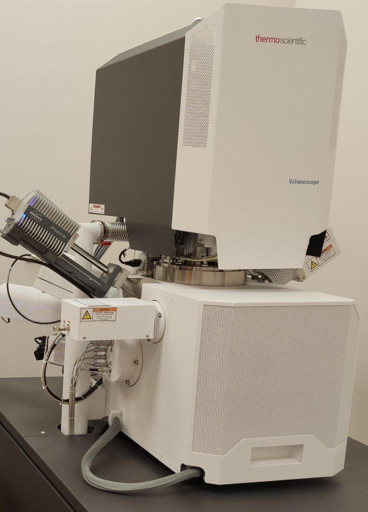
creates an image by detecting reflected or knocked-off electrons. SEM uses a specific set of coils to scan the beam in a raster-like pattern and collect the scattered electrons. Accordingly, SEM provides information on the sample’s surface and its composition with a 3D projection of the samples. EDX spectroscopy to identify the chemical composition of samples is a common practice used in SEM systems. It is important say that SEM sample preparation is relatively easy and its can be directly imaged by mounting them on an aluminum stub. The Thermo Scientific Apreo is a high resolution SEM capable of operating in low vacuum conditions. This microscope is equipped with a VolumeScope Serial Block Face system. This consists of an ultramicrotome mounted inside the vacuum chamber of the SEM which enables cut of ultrasections and finally, after acquisition the interpretation of the 3D architecture of cells and tissues.
Staff:
- Łukasz Mielańczyk, MSc
- Prof. Romuald Wojnicz, MD, PhD
Laboratory services
The laboratory is mainly focused on X-ray microanalysis and high resolution array tomography using both VolumeScope and ARTOS 3D. Similarly to TEM Lab, SEM Lab is mainly focused on applied research.
Equipment
Thermo Scientific VolumeScope

Main features of Thermo Scientific VolumeScope based on Apreo SEM:
- Field Emission Gun (FEG) operating in a range from 200 V to 30 kV, with current amperage from 1 pA up to 400 nA,
- analysis of non-conducting materials under low vacuum conditions with
a maximum pressure of 500 Pa, - electrostatic and electromagnetic lenses that give the possibility to analyze
a wide range of samples, including magnetic ones, - stage biasing from – 4000 V to + 600 V, which improves signals in detectors, especially for non-conductive samples,
- active drift compensation,
- in-situ serial block-face imaging with a demountable ultramicrotome gives the possibility to obtain 3D architecture of cells and tissues in their natural context with isotropic resolution at 10 nm level,
- MAPS software for automated acquisition of high-resolution images from large areas with an Array Tomography module.
Versatile detectors for sample analyzes depend on needs, including:
- Everhart-Thornley Detectors (ETD) for Secondary Electrons,
- Retractable Directional Backscatter (DBS) detector with either annular signals (ABS) or concentric signals (CBS) for topographical backscatter imaging and enhanced composition contrast, respectively,
- Retractable transmitted electrons STEM detector dedicated for TEM grids analysis,
- In-lens T1 and T2 detectors for Backscattered Electrons and Secondary Electrons, respectively,
- Bruker XFlash 6-30 EDS detector:
- with energy resolution as follows: 123 eV at Mn Kα, 45 eV at C Kα, and 53 eV at F Kα,
- extremely high pulse load capability,
- excellent light element and low energy performance (Be – Am element range).
- Bruker XFlash FlatQUAD 5060F detector:
- energy resolution of 126 eV at Mn Kα and 100,000 cps input count rate (51 eV at C K and 60 eV at F K),
- 60 mm2 active area,
- maximum input count rate > 2 million cps,
- excellent light element and low energy performance (Be – Am element range),
- ultrafast mapping with low current,
- dedicated for i.a.: 1. beam sensitive samples, 2. samples with low x-ray yield, 3. mapping of topographic surfaces.
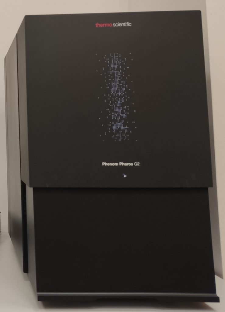
Thermo Scientific Phenom Pharos G2 Desktop FEG-SEM

The main features of Thermo Scientific Phenom Pharos G2:
- Field Emission Gun (FEG) with an adjustable voltage between 1 kV and 20 kV,
- three different vacuum modes: high, medium, and low,
- Back Scattered Electrons (BSE) Detector and Energy-dispersive X-ray spectroscopy (EDS) detector,
- electron-optical magnification range up to 2 000 000x,
- resolution: 3 nm at 20 kV.